CFS End to End NPI Solutions
CFS streamlines your new product introduction procedure from concept to market-ready products.
20+
Inspection equipment
10+
Engineers
5
Month product launch
Common Challenges in New Product Introduction
It is a complex process to bring a new product to the market, and your team may encounter critical obstacles at different stages.
Design vs. Manufacturability Gap
Weak DFM output can make PCB layouts unsuitable for SMT or wave soldering and raise the risk of component damage during board separation.
Unstable Supply Chain
Designers did not consider the supply chain when selecting components, resulting in unstable delivery times for critical components, a lack of alternative materials, and significant batch-to-batch variations.
Material & Process Unfamiliarity
Designers may be unable to combine specialized materials and manufacturing processes, leading to excessively high manufacturing costs or project delays.
Insufficient testing and verification
Due to rushing to market or designers’ lack of experience, LTC, environmental, and ESD testing were not conducted, resulting in high market complaints and return rates.
Certification Risks (UL/EN Failure)
Failure to strictly adhere to certification requirements during sensitivity testing may result in substandard alarm curves, leading to retesting and delays in market launch.
Disorganized project management processes
Due to unclear EVT/DVT/PVT milestones and disorganized change notification (ECN) management, the project was delayed, and costs became uncontrollable.
Providing Seamless Solutions for Every Milestone
From initial concept to final product launch, CFS is here to support you every step of the way.
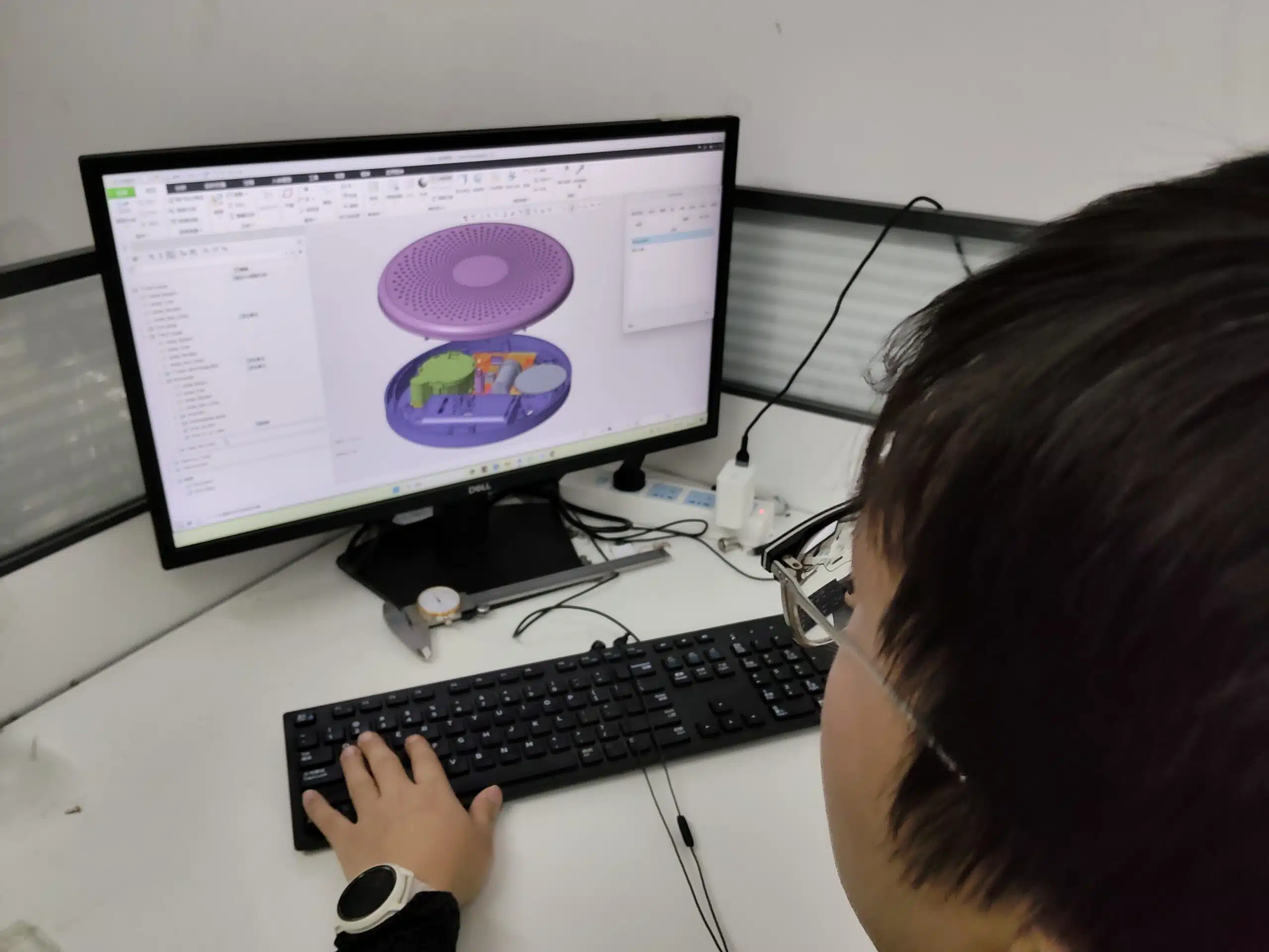
Our R&D Team Expertise
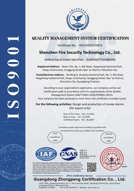
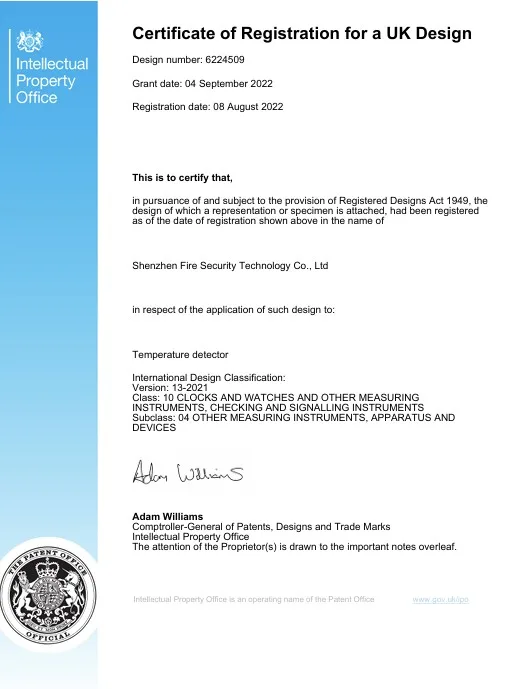
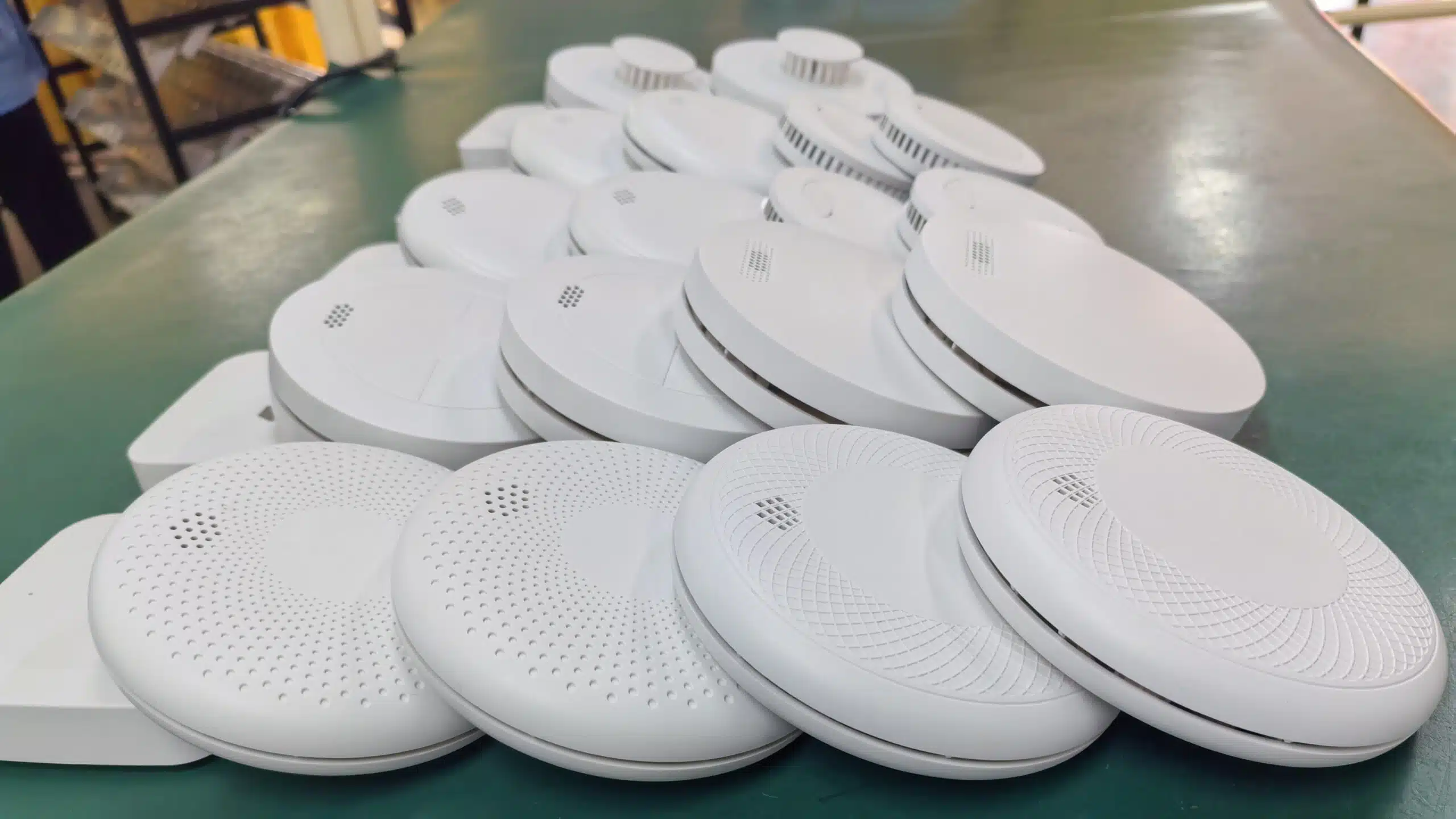
Our R&D team consists of 5 circuit engineers, 3 structural engineers, 2 software engineers, and 1 test engineer, all with over 10 years of experience in smoke and CO detection. We won a Red Dot Design Award in 2025, hold over 10 utility model patents, and have products that have passed multiple international certifications, including UL and EN.
Over the past three years, we have developed 12 new alarm products, with an average development cycle of 5 months per product. We support ODM/OEM production and have delivered over 10 million customized products to date. Our team is market-demand oriented, and new product development goes through six stages, from concept design and prototype manufacturing to certification and mass production, with full control. We launch an average of 5 new alarm products annually for different scenarios, providing customers with reliable and compliant solutions.


12
New Products Developed
(Past 3 Years)
5
Months Average
Development Cycle
10M+
Customized Products
Delivered
5
New Products Launched
Annually
Program Possibility
The project team (including the manager, the electronics engineer, the PCB layout engineer, the mechanical engineer, the firmware engineer, and the validation engineer) discusses and establishes key requirements and creates a draft ATOR and a Product Specification, including:

The project team will conduct a concept design review of the original circuit schematics, 2D drawings, and 3D drawings.
Planning and Requirements Definition
1. Design review and improvement
The project team reviews and improves the circuit schematics, PCB Layout diagrams, 2D and 3D drawings, firmware, other design materials, and certification checklist results.
2. Design engineer completes the Critical Component List based on design theory, BOM, and Sourcing Plan.

3. The project team updates the information as follows:
DFMR(Design for Manufacturing & Reliability)
1. Design engineers release the following documents for DFMR based on the latest product design and prototypes.
2. Sourcing Engineer purchases new and LLT (long lead time) components for each model, which will be used for EVT, DVT, and PVT(PP).
3. The project team completes the DFMR process and provides process issues with a corrective action plan and FPY with defect analysis within 3 days after the DFMR is completed.
4. Design engineers perform bench testing to verify the basic function with the DFMR samples, like the Directionality test, EMI test, and Power testing.
5. The project team completes the component and system FMEA and reviews the draft DFMEA. The DFMEA is a living document and needs to be updated when any design changes are made.
5. Test Protocol Draft
The project team drafts the Component Reliability Test Protocol, System Reliability Test Protocol, and Pre-Agency Test Protocol based on the Product Specification, Agency Standards, and <Product Reliability Test Evaluation Items Instruction>.
EVT(Engineering Validation Test)
1. The project team conducts the EVT build and completes the process report, including process issues with a corrective action plan and FPY with defect analysis within 3 days after EVT is completed.
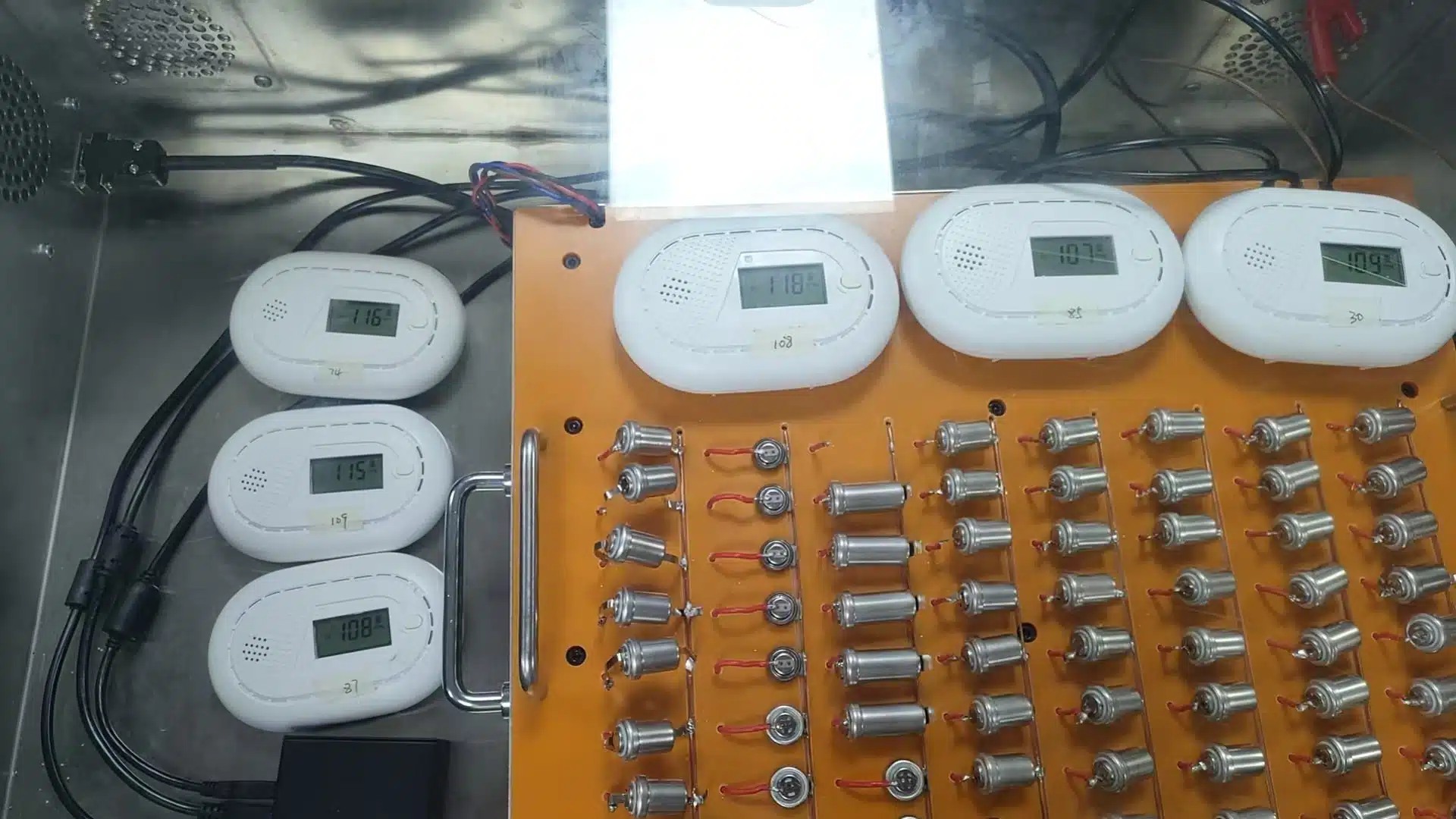
2. Quality engineers arrange Component Reliability Test, System Reliability Test, and Pre-Agency Test in the internal lab and the external lab.
3. The project team reviews the EVT test data based on the Test Protocol, Product Specification, and the agency standard of the product. The design engineers improve the product design based on the EVT test results.
4. Project team completes the process flow chart and defines the quality control points and defines the control method.
5. Project team completes the Process FMEA and updates it when any design or process changes are made.
Certification Preparation
1. The compliance engineer gets the Certification Test Plan and Agency Quote from the agency.
2. The design engineers screen out agency approval samples from EVT based on agency standard requirements and conduct tests.
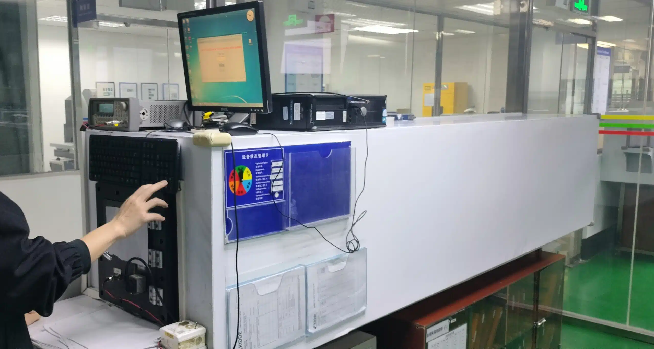
3. Prepare engineering documents for agency approval, including:
4. The electronic engineer arranges smoke sensitivity samples with the agency for a smoke sensitivity test, to seek a correlation for smoke sensitivity between the CFS smoke box and the agency’s smoke box (fire room). To utilize the correlation to specify the smoke sensitivity window for mass production.
5. The PM releases PCN to record the configuration of the agency samples, including BOM, PCB version, circuit diagram version, firmware version, and mechanical drawing version.
6. The project team updates or completes the information as follows:
DVT (Designing Validation Test)
1. Design engineers release the latest documents for the DVT build.
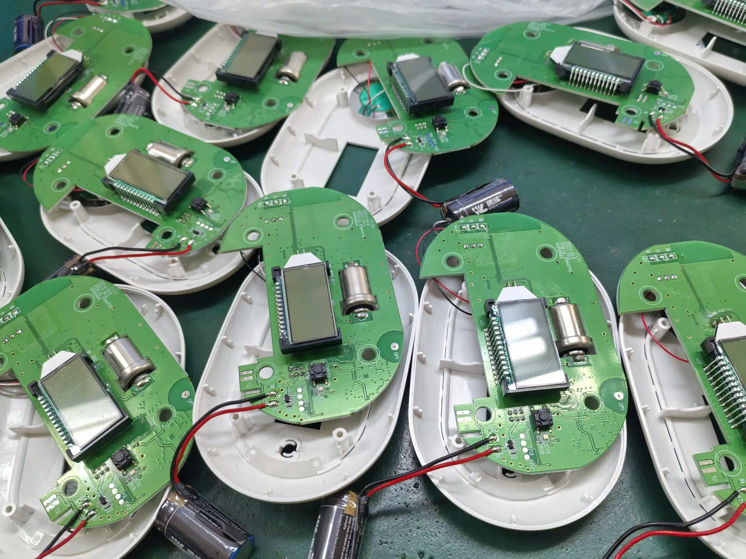
2. The test engineer does the tester qualification and completes the GRR with the project team.
3. DVT build
Process engineers provide the process report, including process issues with a corrective action plan and FPY with defect analysis within 3 days after DVT is completed.
4. DVT Test
Quality arranges component and system reliability tests in the internal lab and external lab.
5. Packaging engineer completes the artwork and structure design based on agency requirements and reviews the new product packaging design with the project team.
6. The design engineers complete the PPAP for new parts.
PP/PVT(Production Pilot)
1. Production Pilot Preparation
Design engineers complete all packaging material PPAP and release the BOM and documents with ECN for the PP build.
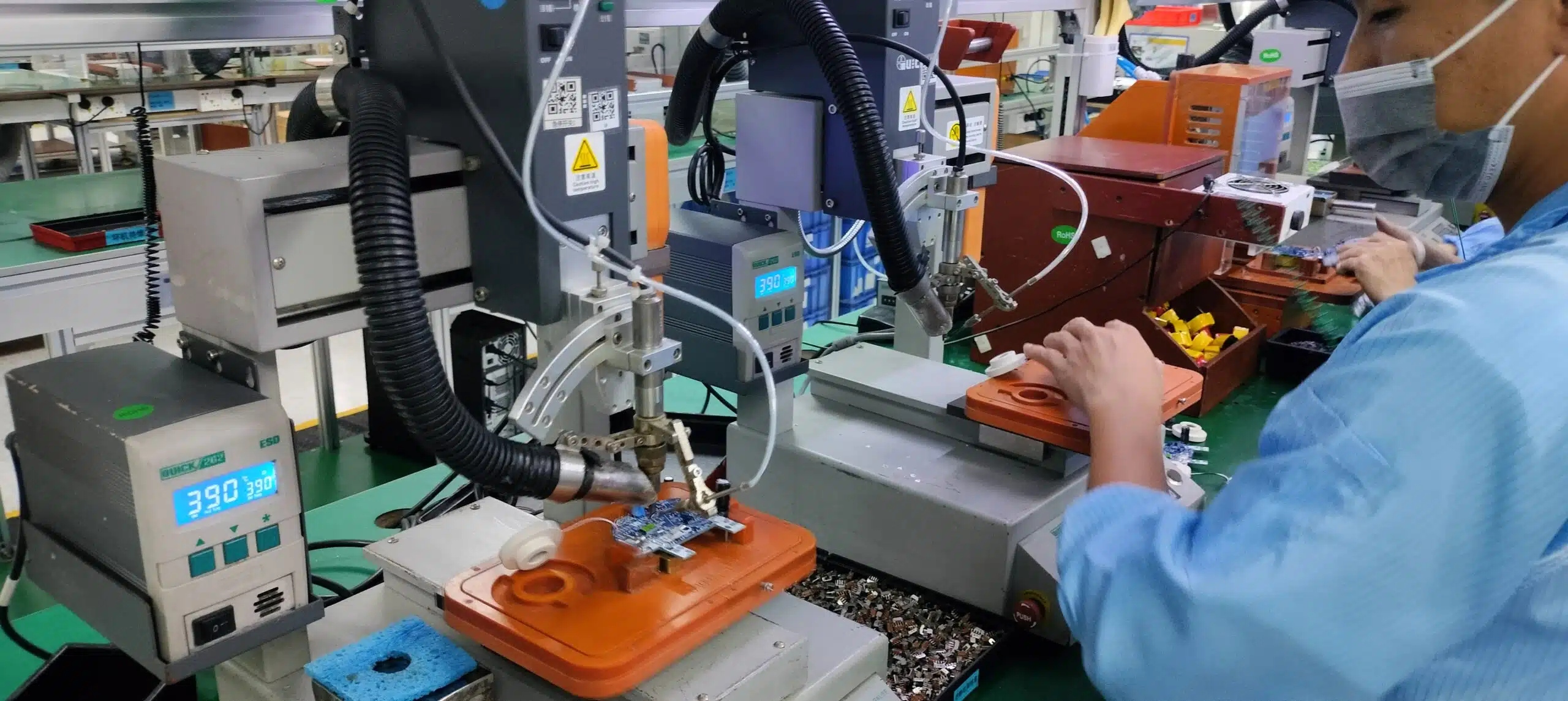
2. Production Pilot
Process engineers lead and complete the Production Pilot with other project members. Process engineers provide the process report, including process issues with a corrective action plan and FPY with defect analysis, within 3 days after PP is completed.
3. Project team releases the process flow chart, MPI, OPC, and the control plan.
MP(Mass production)
Our team collects the marketing feedback after launching the product 12~18 months, reflects on the product features, further evaluates its reliability, cost against original goals, and sums up experiences to apply to future design processes.

Why Choose CFS NPI Solutions
Beyond simple manufacturing—we provide systematic quality control from design to product lifecycle management
Engineering Lead NPI System
At the beginning of the project, we conduct DFM (Design for Manufacturing) reviews, DFT (Design for Test) optimization, and selection of alternative solutions for key components.
Certification-Oriented Design
Certification requirements are thoroughly addressed during the product design phase, and certification itself merely serves as a verification process for the product.
Mature Supply Chain System
Stable AVL system to control raw material stability through PPAP and multi-source procurement of key components during certification phase.
Complete Validation Testing
During the NPI phase, we perform 80+ complete validation tests, including sensitivity testing, LTC stability, environmental aging, ESD and abnormal condition testing.
End-to-End Traceability
We achieve end-to-end MRN/MO/SN traceability from raw material warehousing to shipment.
Standardized NPI Management
We use a milestone management approach: EVT → DVT → PP/PVT → MP with full control at each stage.
Start Your New Product Development Project
Get free consultation, customized solutions, and cost assessment. Our team is ready to help you bring your concept to market.